음, 그런가요.
Here is a summary and analysis of the provided text, broken down for clarity:
Summary of the Article's Core Points
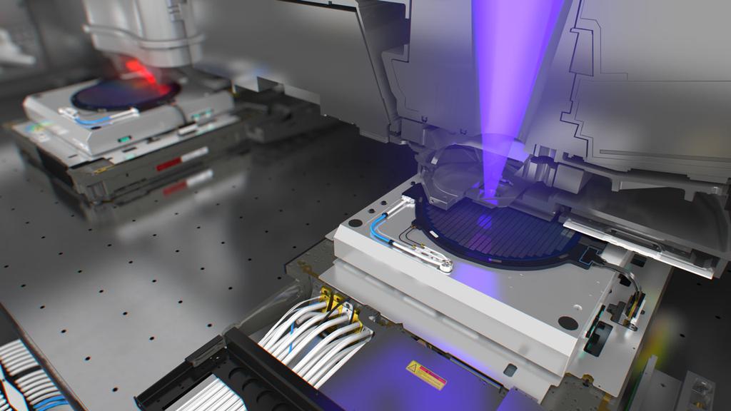
The article discusses the state of China's effort to achieve self-sufficiency in advanced semiconductor manufacturing equipment, specifically focusing on Extreme Ultraviolet (EUV) lithography. The core message is one of significant ongoing effort, substantial technical hurdles, and a gap between ambition and current capability.
Key Takeaways:
- Focus on EUV: China is highly motivated to replicate and advance EUV lithography, a technology critical for producing advanced chips.
- Staggered Progress: While there are signs of localized success (e.g., building components), the entire end-to-end system remains profoundly complex.
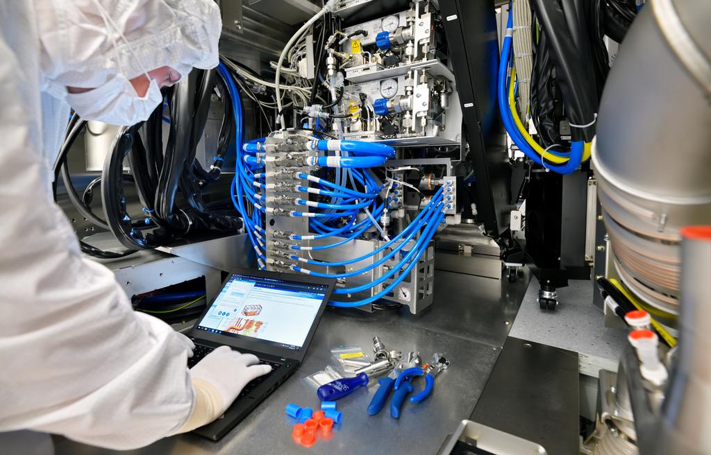
- Hardware vs. System Integration: The difficulty isn't just building individual parts; it's integrating all subsystems (source, optics, etc.) to work together reliably at a commercial, high-yield level.
- Immense Gaps: Foreign technology leaders (like ASML) maintain a massive technological lead across multiple critical subsystems.
- Pace of Development: Efforts are proceeding, but the path to mass production capability is long and fraught with difficulties.
Detailed Analysis and Interpretation
1. The Nature of the Challenge (The "Chasm")
The article highlights that the challenge is systemic, not merely incremental.
- Component Replication vs. System Performance: Simply copying the mechanical or electronic blueprints of a machine is insufficient. A functional lithography machine requires perfect synchronization across multiple domains (vacuum physics, laser physics, ultra-precise optics, etc.).
- "Black Box" Complexity: Foreign leaders operate with decades of cumulative, proprietary knowledge that is incredibly hard to deconstruct and replicate.
2. Technological Hurdles Pointed Out
The text implicitly and explicitly points to several major hurdles:
- The Source: Generating the EUV light source itself is technically demanding.
- The Optics: Developing the complex, multilayered mirrors and lenses that handle EUV light without degradation is a monumental challenge.
- Yield and Reliability: The ultimate measure of success in semiconductor manufacturing is yield (the percentage of functional chips produced). A prototype that works once in a lab is useless if it breaks down after 10 minutes of continuous operation.
3. Context and Implication
The article functions as a geopolitical assessment:
- Self-Reliance Drive: China's focus is framed by national security and technological self-sufficiency goals, making the push relentless.
- Gap Remains Wide: Despite the intense focus and investment, the comparison between domestic capabilities and the established leaders (e.g., ASML) shows a substantial gap that requires significant time and breakthroughs.

In Simple Terms (The "Elevator Pitch")
"China is throwing everything it has at catching up in EUV lithography, which is the core technology for cutting-edge chips. They are successfully building and testing individual parts, which is a huge step. However, the problem isn't just building the parts; it's making all the super-complicated parts talk to each other perfectly, reliably, and 24/7—a hurdle that the world leaders have decades of secret know-how built up. They are making progress, but the race to build a fully functioning, mass-market machine is still a long, difficult journey."